Chris, G3WOS - July 1993
I don't think I could ever, hand on heart, recommend that anyone build a high power solid-state amplifier rather than one based on trusted tetrodes such as the 4CX250B. However, if you read such excellent books such as the recently released ‘The VHF/UHF DX Book’ (DIR Publishing) you will read chapter and verse on actually how difficult it is even getting a valve based amplifier both acceptably linear and reliable. The secret is the same for both valve and transistor; more effort and expense is needed in building the protection circuitry and the power supply than the amplifier itself.
The design presented here is no different. Building a 1 kilowatt power supply that is capable of deliveries 50 volts at 20 amps safely and reliably is no simple task. I also recommend (after building many solid-state amplifiers over the years) that you resist testing and airing your recently completed amplifier until you have built protection circuitry that can detect a high antenna SWR and immediately close down the amplifier. Circuitry is also needed to provide air ALC (automatic linearity control) function to prevent anti-social over-drive splatter. The design presented here is not for the faint hearted or for someone that does not wish to spend, what some would consider, a large amount of money. The BLW96 transistors used in the design cost around Ł100 each and need to be treated carefully. One of my pet hates in any magazine is to see a patronising attitude towards readers, so I will not labour these points excessively! This article does not include the design of the protection circuitry but if I receive sufficient requests, I would be willing to provide details for the next issue of SIX NEWS.
The amplifier uses transistors that have been designed for VHF SSB operation. The 'HF' aspect is important because, unlike VHF devices, they are considerably more stable and do not have that disastrous tendency to go into VHF' parasitic oscillations A possible downside of this is that they may not have less gain at 50MIlz compared to a VHF transistor but, as can be seen in Figure 1, at least 12 to 14dB of gain can be obtained at 50MIlz (the BLW96 performs well at 70MHz as well incidentally). The 'SSB' aspect is important in that the transistor has been designed for linear use and is sold with known inter-modulation performance, unlike most VHF devices that have been designed for FM use. 'The performance of these VHF devices in linear use is questionable, especially so if driven to their power limit.
It is oft quoted that transistor amplifiers have worse IMD performance that valve amplifiers; this is nonsense. The Philips BLW96 is rather an old device by modern standards, but it can be seen in Figure 2 that at 200 - 250 rd watts output it has an 3 order IMD of better than -40dB. This compares very well against any well designed valve amplifier. (It is interesting to note that in common with most transistors, the 3rd order IMD increases as power is reduced, so don't assume that the best performance is achieved by considerably under driving!).
To achieve the required output in this design, two BLW96s have been paralleled to provide 450 watts with just a little over 20 watts of drive. The input power is split using a Wilkinson power divider whose design was extensively discussed in SIX NEWS #33, The output of the two amplifiers are combined using the same, only reversed, circuit. Under normal circumstances the 100 ohm resistor connecting the two output (or input) ports does not dissipate very much power, but during tune-up it is possible that it could. As it is important that these resistors are truly non-inductive, the design uses rather special devices. These are 'bolt-down' 100 Ohm terminating resistors with two flying leads to connect to the circuit board - they look rather like transistors in construction. These are available from Aspen Electronics in Ruislip, UK.
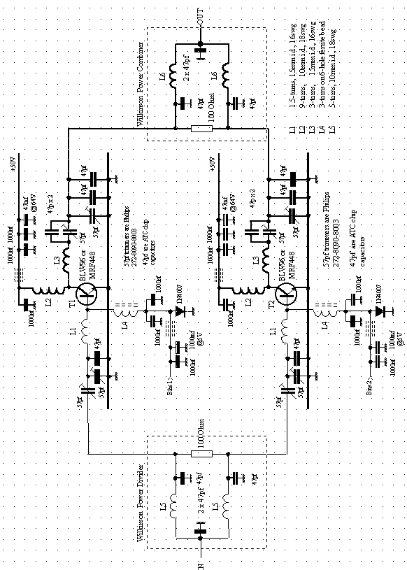 |
Figure 3 - The Circuit Diagram |
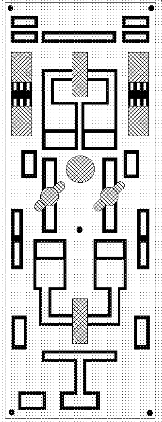
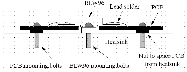
As shown in Figure 3, the two amplifiers use quite conventional low-pass L-matching circuits to match to the 50 Ohm inputs and outputs of the Wilkinson power splitter/combiner. 'the design of these circuits is beyond the scope of this article has been covered elsewhere. What I would like to concentrate on is physical design issues that need to be taken into consideration when building an amplifier of this power. Figure 4 shows the PCB layout at half full size. To reproduce, just pass it through a photocopier on x2 Figure 4 -PCB at 1/2 Full Size magnification. The length of the board should be 27 cm. The PCB uses standard double-sided copperclad board. The cross-hatched areas are cut out holes in the PCB to allow the BLW96s, bias transistors, thermostat, and the power splitter resistors to be bolted to the underlying heatsink. The black areas are not etched but cut out using a sharp knife. and a steel ruler. These gaps provide isolation between the pads and the ground plane Bearing in mind the high voltages in the output circuitry especially, make sure they are not less than 2mm wide. A flashover... well I do not need this further! The PCB is mounted on the heatsink as shown in Figure 5. The BLW96 is bolted to the heatsink using 6BA screws and heatsink compound. In this design especially make sure that the transistors are firmly bolted to the heatsink, and that there are no chamfers on the bolt holes. Going from zero to I kilowatt in less than a microsecond presents a rather high thermal and physical stress to the devices!
 |
 |
The bottom of the printed circuit board |
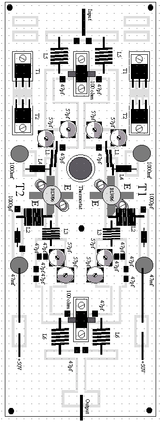
The top of the printed circuit board |
The underside of the PCB is left unetched but must be electrically connected to the upper side ground plane over the full extent of the board. This is achieved by drilling ]mm holes about 10mm apart around all the pads carrying RF power. Short pieces of wire are through these passed through the holes and soldered to both sides of the board (Figure 7). It is especially important to put many of these links around and under the emitters of the BLW96s. The second unusual design technique is shown in Figure 7. The upper and lower ground planes are also shorted together all around the edge of the board. The best way of achieving this is to strip the braid from short lengths of UR-58 coaxial cable and fold this over the edge of the board as shown in Figure 8. Because of the high RF currents circulating in the amplifiers, especially in the output combiner, it is imperative that the correct (or equivalent) fixed and tuning capacitors are used. The ones quoted are low-loss types and do not heat up at all at the power levels encountered in this design. The trimmers are 57pf, Phillips foil trimmers type: 200-80908003 and the 47pf chip capacitors are 300V ATC transmitting types. These look like a small 3mm on-a-side cube.
The PCB is mounted within a large Marston heatsink (available from Famell Components) which is ideally shaped for use as an amplifier (figure 9). The heatsink has two side skirts which provide two sides of the enclosure. The heatsink has a thermal resistance of 0.4o/watt, but as the amplifier dissipates 500 watts at maximum power a fan is needed to keep the heatsink cool. The fan is thermostatically controlled by a small 40o closing thermostatic switch (Marston part #147-092) placed in the centre of the PCB and bolted to the heatsink.
 |
Mounting the Transistors |
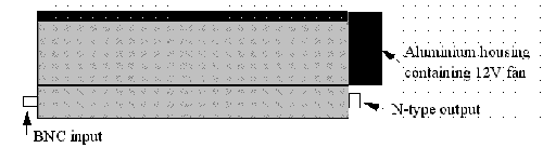
The thermostat controls a small 60mm +48 volt fan which is mounted in Marston heatsink 300mm long, 60DN03000A100, Famell Electronics P148-129 an aluminium enclosure on one end of the heatsink (Figure 10). To force the air through the fins the top of the fins are covered by a piece of aluminium. Two pieces of 10 gauge aluminium sheet are screwed to the ends of the heatsink and an aluminium lid is screwed to the bottom thus fully enclosing the amplifier.
 |
 |
Figure 7 - Wire shorting links |
Figure 8 - Edge shorting links |
The input to the amplifier is via a chassis mounting BNC socket at one end of the housing, while the output is taken via a N-type socket mounted at the other end. Power, 4 50V @ 20A, + 12V for the fan, and switched +50V for the two bias generators are fed in by multi-pole socket. Because of the high RF field inside of the case, all power supply leads that are greater than 10cm long are screened. In the case of the main +50v supply wires, these are screened using 5mm diameter solid brass tube by feeding the multi-strand cable down the centre as shown in Figure 10. A benefit of using brass tube is that the supply wires are held rigidly and neatly in place.
Figure 11 shows the ancilliary circuits for the amplifier. The two bias circuits are driven from a switched +50V supply. The four transistors are bolted to the heatsink as shown in Figure 6. The other components of the bias circuit are mounted on the PCB above, and beside, the transistors. The two 5-watt 100 Ohm resistors are placed against the side wall of the heatsink and held in place with an aluminium bracket. All of the amplifier ancilliary circuitry is be built into a separate cabinet which is connected to the amplifier by a short umbilical cable.
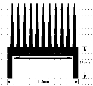 |
Figure 9 - Heatsink Cross-section |
It is recommended that each amplifier is initially tuned individually by disconnecting each in turn from the Wilkinson splitter and combiner and connecting to a 50 Ohm dummy load. Once each amplifier is working correctly, they should be reconnected to the input/output circuitry and final adjustments made. Be very careful at this stage and or) not detune too much. Just move the trimming capacitor a little bit at a time to achieve the required matching. It is all too easy to seriously detune an output circuit which could cause an explosion. Once aligned, and used with a suitable ALC circuit to prevent overload, the amplifier should provide excellent service with IMD performance at as good, or better, than a valve based design. It is interesting to note that I have never seen a need to use phased switching of the power supplies and changeover relays to prevent hot switching.
 |
 |
Figure 10 - Fan housing assembly |
Figure 11 - Screening the 50V supply cables |
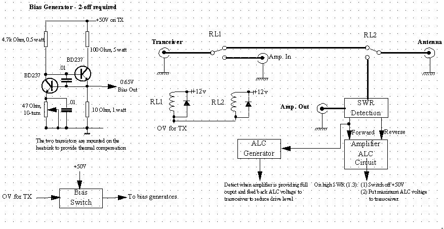 |
Figure 11 - Amplifier Ancilliary Circuitry |
Inspiration for this design came from several sources, the principal one being Dale Harvey, G3XBY, with whom the author has undertaken several VHF amplifier and transverter projects. The second is John Matthews, G3WZT, whose article 'Guidelines for the Design of Semiconductor VHF Power Amplifier' in Sep. 1988 Radio Communication, provided much needed ideas and inspiration.
Although not part of the original article I published in RadCom a possible high power regulator circuit that would form the heart of a 20amp +50V power supply. My original drawing of the circuit is below.
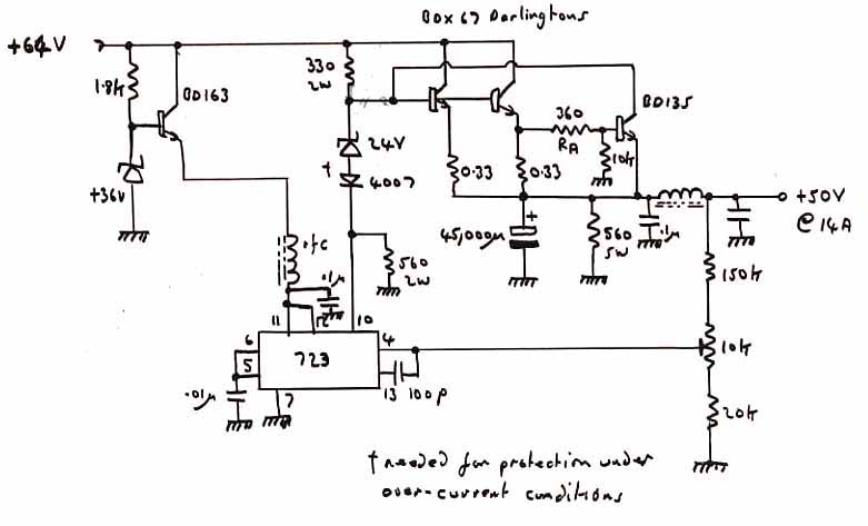 |
| A regular circuit that can be used to create a +50V @ 20 amp power supply. |